Wafer-scale fabrication of graphene for sensing applications (WSGraphene)
The outstanding mechanical and electrical properties of graphene make it an ideal material for the electronics industry for application, particularly for high-speed electronics and sensor applications.
However, despite its high potential, until now it has not been used in practice in the microelectronics industries. This is caused by the fact that the required wafer-scale growth and wafer to wafer transfer of a high-quality graphene layers is very difficult to achieve. This state of affairs is illustrated by the fact that most graphene research groups still get their results by pulling individual micrometer-sized graphene flakes from a graphite block by using Scotch tape: a far cry from an industrially viable process.
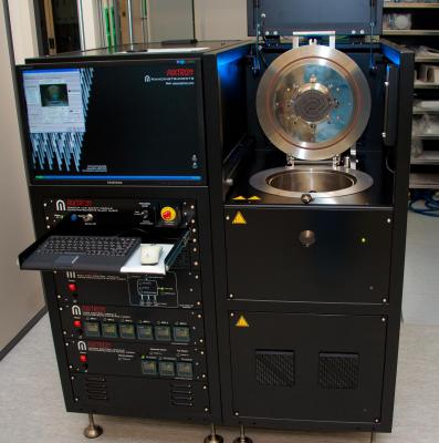
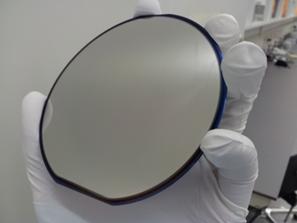
In this project chemical vapour deposition on 10 cm wafers is used to fabricate graphene layers, and transfer techniques are employed to transfer this layer to device wafers. The ultimate goal is to demonstrate that graphene can be integrated in a semi-industrial fabrication process for the fabrication of sensors, bringing the material closer to actual industrial production.
Project data
| Researchers: | Sten Vollebregt, Lina Sarro |
|---|---|
| Starting date: | April 2014 |
| Closing date: | April 2017 |
| Sponsor: | STW |
| Partners: | 3ME, NXP, ASMI, Hauzer Techno Coating, VSL |
| Contact: | Sten Vollebregt |