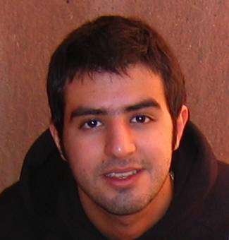
dr. A. Sammak
Electronic Components, Technology and Materials (ECTM), Department of Microelectronics
PhD thesis (Dec 2012): Silicon-Based Integration of Groups III, IV, V Chemical Vapor Depositions in High-Quality Photodiodes
Promotor: Lis Nanver
Biography
Amir Sammak was born in Tehran in 1983. In 2005, He received his B.Sc. and M.Sc degrees in electrical engineering from the University of Tehran, Iran in 2005 and 2007, respectively. During his M.S.c, He has been investigating the fabrication of high-aspect-ratio submicron and nanowire structures. In March 2008, he joined the Faculty of Electrical Engineering, Mathematics and Computer Science at Delft University of Technology, the Netherlands where he is currently working toward the Ph.D. degree. His current research concerns the Epitaxial growth and integration of III-V materials on Silicon substrate.
Publications
- Integrated SiGe Detectors for Si Photonic Sensor Platforms
Gregory Pandraud; Silvana Milosavljevic; Amir Sammak; Matteo Cherchi; Aleksandar Jovic; Pasqualina Sarro;
In Proceedings of Eurosensors,
pp. 559, 2017. - Robust UV/VUV/EUV PureB Photodiode Detector Technology with High CMOS Compatibility
L.K. Nanver; L. Qi; V. Mohammadi; K.R.M. Mok; W.B. de Boer; N. Golshani; A. Sammak; T.L.M. Scholtes; A. Gottwald; U. Kroth; F. Scholze;
Journal of Selected Topics in Quantum Electronics,
Volume 20, Issue 6, pp. pp.1-11, 2014. - A 270�1 Ge-on-Si photodetector array for sensitive infrared imaging
Sammak, A; Aminian, M; Lin Qi; Charbon, E; Nanver, LK;
In Optical Sensing and Detection III Vol. 9141. Proceedings of SPIE- International Society for Optical Engineering,
pp. 1-7, 2014. - VUV/Low-Energy-Electron Si Photodiodes with Post-Metal 400�C PureB Deposition
V. Mohammadi; L. Qi; N. Golshani; K. R. C. Mok; W. B. de Boer; A. Sammak; J. J. Derakhshandeh. van der Cingel; L. K. Nanver;
IEEE Electron Device Letters,
Volume 34, Issue 12, 2013. DOI 10.1109/LED.2013.2287221. - PureGaB p+n Ge diodes grown in large windows to Si with a sub-300 nm transition region
A. Sammak; W.B. de Boer; L. L. Qi K. Nanver;
Journal of Solid-State Electronics,
Volume 74, Issue 1, pp. 126-133, Aug. 2012. DOI 10.1016/j.sse.2012.04.023. - A Ge-on-Si single-photon avalanche diode operating in Geiger mode at infrared wavelengths
M. Aminian; A. Sammak; L. L. Qi K. Nanver; E. Charbon;
In Proc. SPIE: Advanced Photon Counting Techniques VI,
Baltimore, Maryland, Apr 2012. DOI 10.1117/12.920561. - Ge-on-Si: Single-crystal selective epitaxial growth in a CVD reactor
A. Sammak; W.B. de Boer; L.K. Nanver;
In Electro-Chemical Society (ECS) Meeting Abstracts,
Honolulu, Hawaii, Oct. 2012. - Pure dopant deposition of B and Ga for ultrashallow junctions in Si-based devices
L.K. Nanver; A. Sammak; V. Mohammadi; K.R.C. Mok; L. Qi; A. Sakic; N. Golshani; J. Derakhshandeh; T.M.L. Scholtes; W.D. de Boer;
In ECS Trans. 2012: 27th Symposium on Microelectronics Technology and Devices (SBMicro2012),
Brazil, Brasilia, pp. 25-33, Aug. 2012. DOI 10.1149/04901.0025ecst. - Silicon-based integration of groups III, IV, V chemical vapor deposition in high quality photodiodes
A. Sammak;
PhD thesis, Delft University of Technology, Dec. 2012. ISBN 9789462032705; Promotor: prof.dr. L.K. Nanver. - Large-area selective CVD epitaxial growth of Ge on Si substrates
A. Sammak; W.B. de Boer; L. L. Qi K. Nanver;
In Proc. ICT.OPEN: Micro technology and micro devices (SAFE 2011),
Veldhoven, The Netherlands, pp. 96-99, Nov. 2011.
document - High-quality p+n Ge diodes selectively grown on Si with a sub-300nm transition region
A. Sammak; W.B. de Boer; L. L. Qi K. Nanver;
In Proc. European Solid-State Device Research Conference (ESSDERC 2011),
Helsinki, Finland, pp. 359-362, Sep. 2011. ISBN 978-1-4577-0707-0; DOI 10.1109/ESSDERC.2011.6044160. - A CMOS compatible Ge-on-Si APD operating in proportional and geiger modes at infrared wavelengths
A. Sammak; M. Aminian; L. Qi; W.B. de Boer; E. Charbon; L.K. Nanver;
In International Electron Device Meeting (IEDM 2011),
Washington DC, Dec. 2011. - Merging standard CVD techniques for GaAs and Si epitaxial growth.
A. Sammak; W.B. de Boer; Boogaard; A van den; L.K. Nanver;
ECS Transactions,
Volume 28, Issue 5, pp. 237-244, 2010. - Unifying GaAs and Si epitaxial growth in a standard Si/SiGe CVD system.
A. Sammak; W.B. de Boer; L.K. Nanver;
In STW-SAFE 2010 Conference Proceeding,
Veldhoven, pp. 147-154, 2010. - Chemical vapor deposition of Ga dopants for fabricating ultrashallow pn junctions at 400
A. Sammak; L. Qi; W.B. de Boer; L.K. Nanver;
In 10th IEEE International Conference on Solid-State and Integrated Circuit Technology (ICSICT 2010),
Shanghai, China, pp. 969-971, 2010.
document - Chemical Vapor Deposition of Gallium on Silicon and SiO2. In PJ French
A. Sammak; W.B. de Boer; L.K. Nanver; L. Qi; G. Lorito;
In Proc. of SAFE 2009,
Veldhoven, The Netherlands, pp. 538-541, 2009.
document - Hyrogenation Assisted Lateral Micromachining of (111) Silicon Wafers
S. Darbari; S. Azimi; S. Mohajerzadeh; A. Sammak; N. Izadi; S. Famini;
IEEE Journal of Microelectromechanical systems,
Volume 17,, Issue 6, pp. 1489-1494, Dec. 2008. - On the Aluminum-Mediated Solid-Phase Epitaxy of Silicon at 300C
A. Sammak; Y. Civale; L. K. Nanver;
In Proc. 11th Annual Workshop on Semiconductor Advances for Future Electronics and Sensors (SAFE),
Veldhoven, The Netherlands, Nov. 2008. - Deep vertical etching of silicon wafers using a hydrogenation assisted reactive ion etching
A. Sammak; S. Azimi; N. Izadi; B. Khadem Hosseinieh; S. Mohajerzadeh;
IEEE Journal of Microelectromechanical Systems,
Volume 16, Issue 4, pp. 912-918, Aug. 2007. - Smart etch or plasma hydrogenation-assisted high aspect ratio etching of silicon
S. Azimi; A. Sammak; B. Khadem Hosseinieh; S. Mohajerzadeh; R. Faez; N. Izadi;
In ICEE 2007,
ITRC, Iran, 2007. - Silicon Nanowire Fabrication Using Novel Hydrogenation-Assisted Deep Reactive Ion Etching
A. Sammak; S. Azimi; B. Khadem Hosseinieh; S. Mohajerzadeh; E. Asl Soleimani;
In ISDRS 2007,
College Park MD, USA, Dec. 2007.
BibTeX support
Last updated: 9 Mar 2019

Amir Sammak
Alumnus- Left in 2012
- Now: TNO-QuTech
- Google Scholar profile