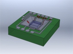
3D Smart Wafer Level Package for LEDs (SmartPackage)
Besides the increasing use of LEDs for various application, there are different reliability issues for LED systems such as change in brightness and colour temperature due to high working temperature and aging. So system performance monitoring and further control options become more essential. In addition Silicon based wafer level packaging can be a promising way to integrate different smart functions to LED system and furthermore use wide benefits of silicon technology.
To address such issues in this project a new monolithic package is introduced. All the steps are just done in few mask step BiCMOS process, which is optimized for performance of different passive and active components. To monitor the system performance, temperature and light sensing elements are integrated. To control the performance of the package light feedback and sensor readout circuits are designed and fabricated. This process flow integrates simultaneously the photodiodes, the CMOS and BJT transistors and feedback and sensor readout circuits.
This IC includes several functional devices for a smart wafer level LED packaging. In 3D version of the package the Aluminum coated cavity is used as a local reflector cup and high aspect ratio interconnects are used for supplying LED power. Having different kind of sensors in the same package with LED chips and readout circuit can be an appropriate demonstrator for different applications such as biomedical diagnostic devices.

Project data
| Researchers: | Zahra Kolahdouz Esfahani, Teng Ma, Henk van Zeijl, GuoQi Zhang |
|---|---|
| Starting date: | October 2011 |
| Closing date: | October 2015 |
| Sponsor: | EU ESiP |
| Contact: | GuoQi Zhang |