Gallium nitride (GaN) on silicon system integration (GaNonSi)
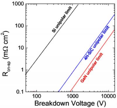
Si-based power devices have reached maturity and are approaching their physical limits of operation. Implementation of new wide-bandgap (WBG) semiconductor materials is necessary to achieve higher efficiencies with increased power densities. GaN is a promising material for power electronics due to its wide bandgap (3.4eV), high critical electric field (3-4MV/cm) and low intrinsic carrier concentration with electron mobility and thermal conductivity values comparable to Si. Due to limited availability of bulk GaN substrates, heteroepitaxial growth on non-native SiC, sapphire or Si wafers needs to be used. The advantage of Si over other substrates is low-cost, integration with other IC processes and high diameter substrate availability.
In this project, we will focus on design and fabrication of GaN power devices (HEMT, Schottky diodes, rectifiers) on large diameter (6-inch) Si substrates. We will explore the possibilities to integrate these components with embedded passives, MEMS or CMOS components for higher value system-in-package (SiP) for power conversion and high frequency amplifier applications.

Project data
| Researchers: | Robert Sokolovskij, Fabio Santagata, Mingzhi Dong, Elina Iervolino, GuoQi Zhang |
|---|---|
| Starting date: | January 2014 |
| Closing date: | January 2017 |
| Sponsor: | State Key Laboratory of Solid St |
| Partners: | Beijing Research Centre |
| Contact: | GuoQi Zhang |